Richard Feynman is considered one of the fathers of nanotechnology. He did extensive work in atomic physics and made discoveries of the extremely small which he presented to the American Physical Society on December 29, 1959, at Caltech. The presentation title was, “There's Plenty of Room at the Bottom.” In this presentation, Feynman extended an invitation for scientists to begin manipulating and controlling things on a small scale, thereby entering a new world of physics. He proposed several concepts including writing at the nanoscale, building nanomachines and creating methods for fabrication, as well as storing digital information at the nanoscale. Feynman's presentation spurred the development of a new field of science called “nanoscience”.
Scroll through the history of nano. Tap an image to explore.


Norio Taniguchi of the Tokyo Science University, a Japanese production engineer devoted to accuracy and precision, coined the term nanotechnology in 1974. His definition referred to a production technology that ensured superior accuracy and ultra-fine dimensions on the order of 1 nanometre. The modern understanding of nanotechnology was defined years later as “the creation of functional materials, devices and systems through control of matter on the nanometre length scale (1-100 nanometres), and exploitation of novel phenomena and properties (physical, chemical, biological) at that length scale.”
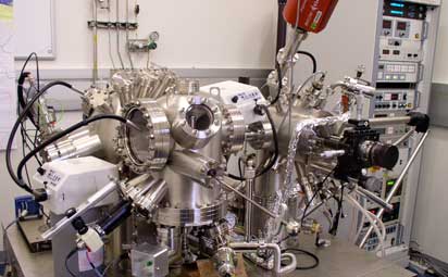
The first scanning probe microscope, the scanning tunnelling microscope (STM), was invented by Gerd Binnig and Heinrich Rohrer in 1981. Scanning Probe Microscopes (SPM) feel across the surface of a sample with a tip so sharp it contains only one atom. The distance between the tip and the surface is measured to visualize the tiny features of the sample. The only limitation is that an STM can only image conducting surfaces since electric current is used to create the image.
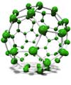
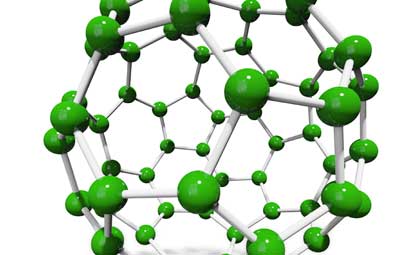
In September 1985, a new kind of carbon family was discovered by three innovative chemists, Robert F. Curl, Sir Harold W. Kroto, and Richard E. Smalley. They worked together at Rice University in Houston, Texas, to perform a set of experiments and discovered a hollow, spherical, 60 carbon containing molecule that was very different and much harder than graphite and diamond. It was officially named Buckminster fullerene (in honour of R. Buckminster Fuller who designed and built the first geodesic dome), but is commonly known as a buckyball.
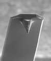
Gerd Binnig (of the STM discovery), Christoph Gerber, and Calvin Quate invented the first atomic force microscope (AFM) in 1986. The AFM is a type of Scanning Probe Microscope that creates nanoscale images by “feeling” the surface with a mechanical probe. The tip is so sharp that a single atom forms the point, and this atom is placed close enough to the sample that atoms on the surface of the sample interact with the tip providing an image. The AFM is one of the foremost tools for imaging, measuring, and manipulating matter at the nanoscale. While the resolution is not as high as a STM, the AFM has the benefit of being able to image both conducting and insulating surfaces.


Quantum dots were discovered in the early 1980's by Alexei Ekimov and Louis E. Brus. Quantum dots are nanometre sized metallic or semi-conductive particles. These quantum dots can be used to store electrons, or to transform the color of light. Electronic characteristics of quantum dots are closely related to the size and shape of the individual crystal, which can be grown in a controlled way to precise dimensions. Generally, the smaller the size of the crystal the more energy is needed to excite the dot and subsequently the more energy is released when the crystal returns to its resting state. Researchers are studying quantum dots and potential applications in transistors, solar cells, LEDs, medical imaging, and quantum computing. The term “quantum dot” was created by Mark Reed in 1988.
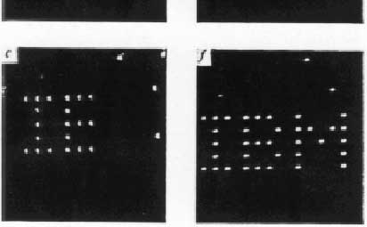
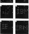
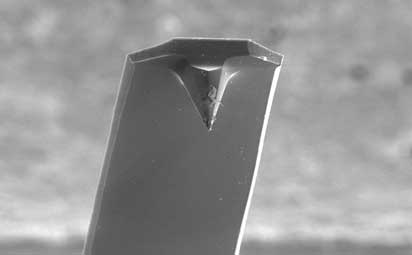
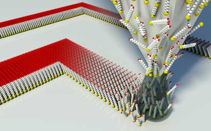
Donald Eigler achieved a landmark in nanoscience by demonstrating the ability to manipulate individual atoms with atomic-scale precision. On September 28, 1989 he wrote IBM using 35 individual xenon atoms at the IBM Almaden Research Center. He wrote this by using a low temperature ultra-high vacuum scanning tunnelling microscope that he designed and built.
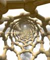
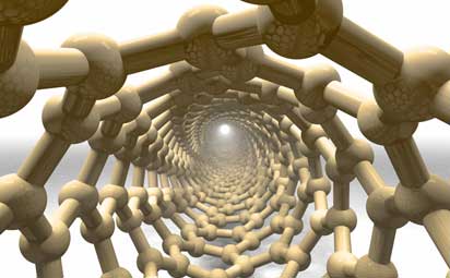
Another form of fullerene, a molecule composed entirely of carbon, was discovered by Sumio Iijima consisting of cylindrical tube-like molecules made up of graphene sheets (a single layer of carbon molecules shaped in connected hexagons, a honeycomb-like pattern). They are extremely strong materials and have good thermal conductivity. Carbon nanotubes are extremely thin (their diameter is about 10,000 times smaller than a human hair). A single walled nanotube (SWNT) is composed of one rolled graphite sheet; if multiple sheets are used they are named multiwalled nanotube (MWNT).
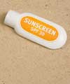
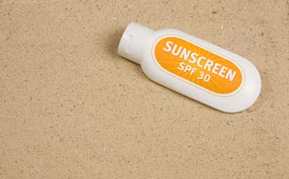
The first generation of nanotechnology containing consumer products was introduced to market in the '90s with isolated applications, such as titanium dioxide nanoparticles in sunscreen. The development of nanotechnology is usually divided into four stages or generations.
- The first generation involves passive nanostructures; the individual nanostructures have interesting properties or interactions with the environment that occur passively (without applied energy or force) and are used together as coatings, nanoparticles, or bulk materials (nanostructured metals, ceramics, polymers).
- The second generation involves active nanostructures; the properties of individual nanostructures are used actively in creating the output of a device through applied energy or force in structures such as transistors, actuators, amplifiers, or nanocrystalline LED's.
- The third generation will consist of three dimensional nanosystems built with different nanocomponents such as in nanosized circuits or sensors.
- The fourth generation will consist of many different nanocomponents working together in a molecular nanosystem, where each molecule in the system has a specific structure and plays a different role.
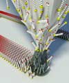
DPN or Dip Pen Nanolithography was developed by Chad Mirkin and coworkers as an “ink” and “paper” approach to patterned self-assembling monolayer's (SAM) on gold. A SAM is a layer that is a single molecule thick and the self-assembly refers to the “ink” molecule on the “pen” sticking to the “paper” surface. This approach involves using the tip of an atomic force microscope as the “pen” to transfer an “ink” such as alkanethiol through capillary action to the underlying gold surface. This technique is currently not rapid enough to be considered for nanofabrication; however, DPN can deliver minuscule amounts of molecules from the AFM tip to the substrate at high resolution and is therefore a promising technique.
We have already begun to see first generation (starting in the early '90s and coming out with many applications starting in 2001), second generation (introduced in 2005), and third generation nanotechnology (2011). These generations have been illustrated in several different commercial applications. Nanomaterials are used to add strength to composite materials in tennis rackets, baseball bats, and bicycles, as well as applied as coatings on fabrics to make them stain resistant or on glass to keep it clean, repel oil, and be scratch resistant. Nanostructered catalysts are used to make chemical manufacturing processes more efficient, saving energy and reducing waste. Almost all electronic devices manufactured in the last decade use some nanomaterials.
Research is ongoing with hopes of introducing nanotechnology-based medicine such as using nanoparticles to deliver drugs directly to the site it is needed or to improve medical imaging tools, like MRIs and CAT scans. Medical diagnostics, with the help of nanotechnology, may soon be used in your doctor's office for fast analysis without having to wait while samples are sent to a lab. The energy industry will use nanocatalysts in fuel cells, nanoparticles in batteries for higher capacity and longer life, and nanomaterials for better solar energy applications. Nanosensors may be used in food packaging to detect germs and spoilage. Building materials will be stronger, lighter, and more durable. The fourth generation of nanotechnology is projected to be introduced as early as 2020, offering manufacturing and fabrication at the molecular level. Perhaps one day we may even see nanorobotic systems with applications such as nanosurgery inside our bodies, even inside our cells. The applications of nanotechnology are limitless, and as our knowledge and technology progresses it is an exciting new frontier of discovery.
- Home
-
Credits

Module 1 : SEM Image Gallery
Images provided by the National Institute of Nanotechnology, University of Alberta
Module 2: Scale of Nano
Exploratorium: Developed for the NISE Network with funding from the National Science Foundation under Award Numbers 0532536 and 0940143.
Module 3: What is Nano?
Dr. Nils Petersen, Director General, NINT, Micralyne
Maziyar Khorasani, VP Business Development, Biolithic CorporationModule 4: Quantum Dot Animation
Video provided by Robert A. Wolkow, University of Alberta
Module 5: The Numbers on Nano
Palmberg, C., H. Dernis, and C. Miguet. 2009. Nanotechnology: An Overview Based on Indicators and Statistics. STI Working Paper 2009/7: Statistical Analyis of Science, Technology and Industry. OECD.
Module 7: Nano in Nature, World's Smallest
Car
Images and video provided by James Tour, Rice University.
Guitar
Images and video provided by Harold Craighead, Cornell University.
Card
Image provided by David Cummings, University of Glasgow.
Snowman
Images and video provided by David Cox, National Physical Laboratory
Map
Image provided by Paul Rothemund, Caltech.
Image and video provided by IBM – Zurich Research.Gecko
Images provided by Kellar Autumn, Lewis & Clark College.
Images provided by Bjorn Christian Torrissen
Video provided by the Anthony Russell, University of Calgary.Lotus
Video provided by Nanoyou, and The research leading to these results has received funding from the European Community's Seventh Framework Programme (FP7/2007-2013) under grant agreement n° 233433.
Beetle
Image provided by Jeremy Galusha, University of Utah.
Moth
Paivanranta, B., T. Saastamoinen, and M. Kuittinen. 2009. A wide-angle antireflection surface for the visible spectrum. Nanotechnology. 20(37): 1-7.
Image provided by Dartmouth Electron Microscope Facility, Dartmouth College